Part A. Physical Layer Specification
vAtlanta r00
This Part describes the Bluetooth Low Energy physical layer.
1. Scope
Bluetooth Low Energy (LE) devices operate in the unlicensed 2.4 GHz ISM (Industrial Scientific Medical) band. A frequency hopping transceiver is used to combat interference and fading.
Two modulation schemes are defined. The mandatory modulation scheme (“1 Msym/s modulation”) uses a shaped, binary FM to minimize transceiver complexity. The symbol rate is 1 Msym/s. An optional modulation scheme (“2 Msym/s modulation”) is similar but uses a symbol rate of 2 Msym/s.
The 1 Msym/s modulation supports two PHYs:
LE 1M, with uncoded data at 1 Mb/s;
LE Coded, with the Access Address, Coding Indicator, and TERM1 coded at 125 kb/s and the payload coded at either 125 kb/s or 500 kb/s.
A device shall support the LE 1M PHY. Support for the LE Coded PHY is optional.
The 2 Msym/s modulation supports a single PHY:
LE 2M, with uncoded data at 2 Mb/s
A Time Division Duplex (TDD) scheme is used on all PHYs. The specification defines the requirements for a Bluetooth radio for the Low Energy radio.
Requirements are defined for two reasons:
Provide compatibility between radios used in the system
Define the quality of the system
An LE radio shall have a transmitter or a receiver, or both.
The LE radio shall fulfill the stated requirements for the operating conditions declared by the equipment manufacturer (see Section A.1).
The specification is based on the established regulations for Europe, Japan, North America, Taiwan, South Korea and China. The standard documents listed below are only for information, and are subject to change or revision at any time.
The Bluetooth SIG maintains regulatory content associated with Bluetooth technology in the 2.4 GHz ISM band on its web site, at https://www.bluetooth.com/regulatory-requirements/.
Europe:
Approval Standards: European Telecommunications Standards Institute, ETSI Documents: EN 300 328, EN 300 440, EN 301 489-17
Japan:
Approval Standards: Japanese Radio Law, JRL Documents: Japanese Radio Law: Article 4.3, Article 28, Article 29, Article 38 Radio Equipment Regulations: Article 5, Article 6, Article 7, Article 14, Article 24, Article 9.4, Article 49.20.1.C.2, Article 49.20.1.E.3 Radio Law Enforcement Regulations: Article 6.2, Article 6.4.4.1, Article 7
North America:
Approval Standards: Federal Communications Commission, FCC, USA Documents: CFR47, Part 15: Sections 15.205, 15.209 and 15.247 Approval Standards: Industry Canada, IC, Canada Documents: RSS-210 and RSS139
Taiwan:
Approval Standards: National Communications Commission, NCC Documents: Low Power 0002 (LP0002); Low-power Radio-frequency Devices Technical Regulations
South Korea:
Approval Standards: Korea Communications Commission, KCC Documents: Rules on Radio Equipment 2008-116
China:
Approval Standards: Ministry of Industry and Information Technology, MIIT Documents: MIIT regulation [2002]353
2. Frequency bands and channel arrangement
The LE system operates in the 2.4 GHz ISM band at 2400 MHz to 2483.5 MHz. The LE system uses 40 RF channels with center frequencies at a 2 MHz spacing from 2402 MHz to 2480 MHz.
3. Transmitter characteristics
The requirements stated in this section are given as power levels at the antenna connector of the LE device; this is also referred to as the radiative transmit power level of the device. If the device does not have a connector, a reference antenna with 0 dBi gain is assumed. Power level values used in HCI commands, HCI events, Advertising physical channel PDUs, and Link Layer Control PDUs shall be assumed to be the radiative transmit power level of the device unless specified otherwise.
Due to the difficulty in making accurate radiated measurements, systems with an integral antenna should provide a temporary antenna connector during LE PHY qualification testing.
For a transmitter, the radiative transmit power level at the maximum power setting shall be between 0.01 mW (-20 dBm) and 100 mW (+20 dBm).
Devices shall not exceed the maximum allowed transmit power levels set by the regulatory bodies that have jurisdiction over the locales in which the device is to be sold or intended to operate. Implementers should be aware that the maximum transmit power level permitted under a given set of regulations might not be the same for all modulation modes.
Using high transmit power in use cases where short ranges could be encountered can cause the receiver on the remote device to be saturated and result in link failure. The LE Power Control Request feature can be used to adjust a connected remote device’s transmit power level based on the receiver’s signal level. When the LE Power Control Request feature is used on a connection with long connection intervals, devices should use reliable RSSI measurements from recent connection events to determine whether or not to send power control requests. When a device is capable of adjusting its transmit power level using the LE Power Control Request feature, the difference between any two adjacent transmit power levels supported by the radio design should be no greater than 8 dB. When the LE Power Control Request feature is not supported by either the local or remote device, implementers should avoid use of high output power in such scenarios or employ a mechanism for switching between two or more transmit power levels in an attempt to establish, re-establish, or maintain connections.
The output power control of a device may be changed locally, for example to optimize the power consumption or reduce interference to other equipment.
Bluetooth devices are classified into power classes based on the output power level at the maximum power setting the LE PHY supports (Pmax), as defined in Table 3.1.
Power Class | Requirements |
|---|---|
1 | 100 mW (+20 dBm) ≥ Pmax ˃ 10 mW (+10 dBm) |
1.5 | 10 mW (+10 dBm) ≥ Pmax ˃ 2.5 mW (+4 dBm) |
2 | 2.5 mW (+4 dBm) ≥ Pmax ˃ 1 mW (0 dBm) |
3 | 1 mW (0 dBm) ≥ Pmax ≥ 0.01 mW (-20 dBm) |
3.1. Modulation characteristics
The modulation is Gaussian Frequency Shift Keying (GFSK) with a bandwidth-bit period product BT=0.5. The modulation index shall be between 0.45 and 0.55. A binary one shall be represented by a positive frequency deviation, and a binary zero shall be represented by a negative frequency deviation.
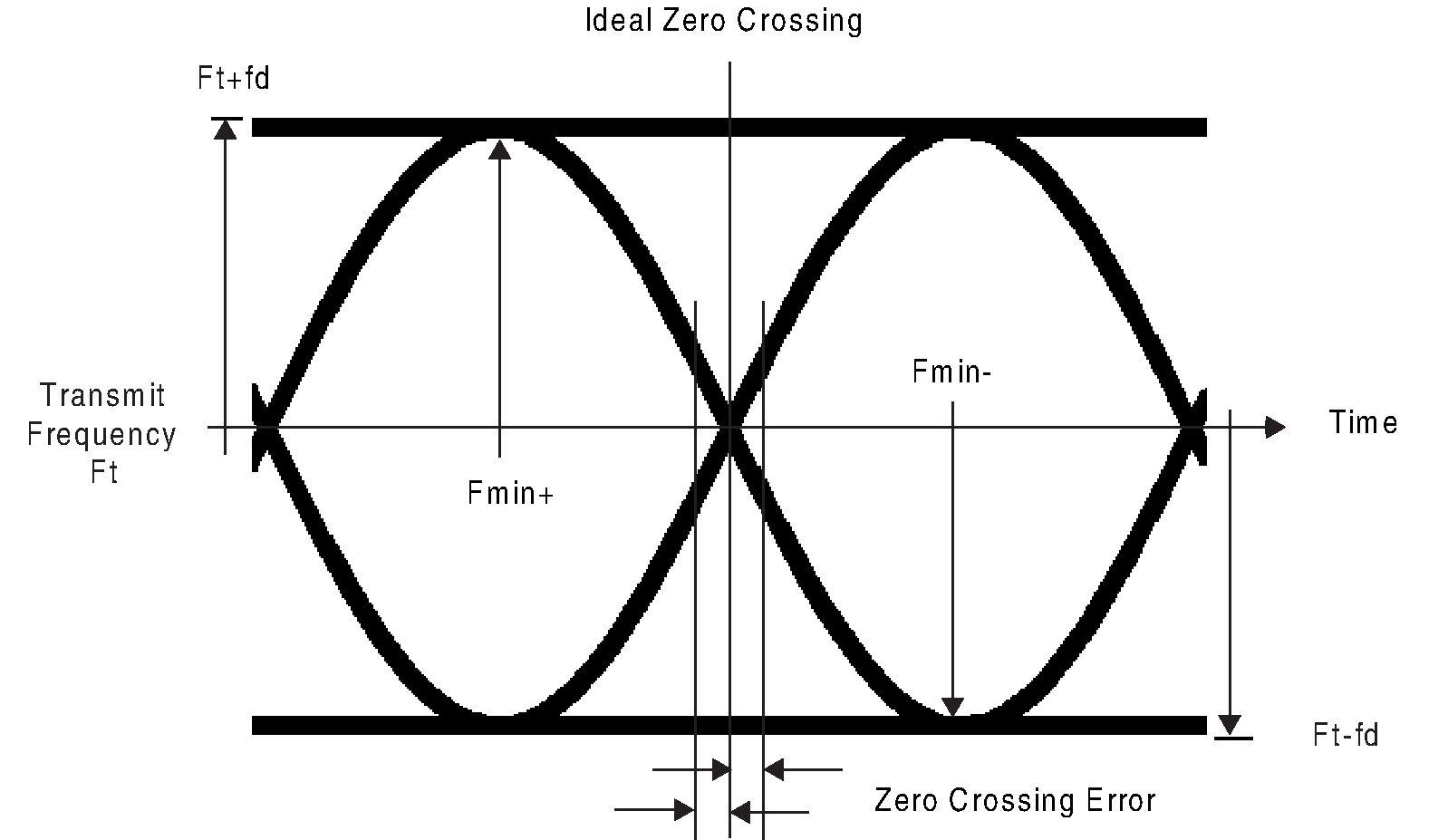
For each transmission the minimum frequency deviation,
which corresponds to a 1010 sequence, shall be no smaller than ±80% of the frequency deviation with respect to the transmit frequency, which corresponds to a 00001111 sequence.
The minimum frequency deviation shall never be less than 185 kHz when transmitting at 1 megasymbol per second (Msym/s) symbol rate and never be less than 370 kHz when transmitting at 2 Msym/s symbol rate. The symbol timing accuracy shall be better than ±50 ppm.
The zero crossing error is the time difference between the ideal symbol period and the measured crossing time. This shall be less than ±1/8 of a symbol period.
See Figure 3.1 for the definitions of some symbols and terms in these requirements.
3.1.1. Stable modulation index
An LE device with a transmitter that has a stable modulation index may inform the receiving LE device of this fact through the feature support mechanism (see [Vol 6] Part B, Section 4.6). The modulation index for these transmitters shall be between 0.495 and 0.505. A device shall only state that it has a stable modulation index if that applies to all LE transmitter PHYs it supports.
A transmitter that does not have a stable modulation index is said to have a standard modulation index.
3.2. Spurious emissions
3.2.1. Modulation spectrum
For products intended to comply with FCC part 15.247 rules, the minimum 6 dB bandwidth of the transmitter spectrum shall be at least 500 kHz using a resolution bandwidth of 100 kHz.
3.2.2. In-band spurious emission
An adjacent channel power is specified for channels at least 2 MHz from the carrier when transmitting with1 Msym/s modulation (applies to the LE 1M and LE Coded PHYs) or at least 4 MHz from the carrier when transmitting with 2 Msym/s modulation (applies to the LE 2M PHY). This adjacent channel power is defined as the sum of the measured power in a 1 MHz bandwidth.
The spectrum measurement shall be performed with a 100 kHz resolution bandwidth and an average detector. The device shall transmit on an RF channel with the center frequency M and the adjacent channel power shall be measured on a 1 MHz RF frequency N. The transmitter shall transmit a pseudo random data pattern in the payload throughout the test.
Frequency offset | Spurious Power |
|---|---|
2 MHz (|M-N| = 2) | -20 dBm |
3 MHz or greater (|M-N| ≥ 3) | -30 dBm |
Frequency offset | Spurious Power |
|---|---|
4 MHz (|M-N| = 4) | -20 dBm |
5 MHz (|M-N| = 5) | -20 dBm |
6 MHz or greater (|M-N| ≥ 6) | -30 dBm |
Exceptions are allowed in up to three bands of 1 MHz width, centered on a frequency which is an integer multiple of 1 MHz. These exceptions shall have an absolute value of -20 dBm or less.
3.2.3. Out-of-band spurious emission
The equipment manufacturer is responsible for the ISM out-of-band spurious emissions requirements in the intended countries of sale.
3.3. Radio frequency tolerance
The deviation of the center frequency during the packet shall not exceed ±150 kHz, including both the initial frequency offset and drift. The frequency drift during any packet shall be less than 50 kHz. The drift rate shall be less than 400 Hz/µs.
The limits on the transmitter center frequency drift within a packet is shown in Table 3.4.
Parameter | Frequency Drift | ||||||||||||||||||||||||||||||||||||||||||||||||
|---|---|---|---|---|---|---|---|---|---|---|---|---|---|---|---|---|---|---|---|---|---|---|---|---|---|---|---|---|---|---|---|---|---|---|---|---|---|---|---|---|---|---|---|---|---|---|---|---|---|
Maximum drift | ±50 kHz | ||||||||||||||||||||||||||||||||||||||||||||||||
Maximum drift rate[a] | 400 Hz/μs | ||||||||||||||||||||||||||||||||||||||||||||||||
[a] The maximum drift rate is allowed anywhere in a packet. | |||||||||||||||||||||||||||||||||||||||||||||||||
4. Receiver characteristics
The reference sensitivity level referred to in this section is -70 dBm. The packet error rate corresponding to the defined bit error ratio (BER) shall be used in all receiver characteristic measurements.
4.1. Actual sensitivity level
The actual sensitivity level is defined as the receiver input level for which the BER specified in Table 4.1 is achieved.
Maximum Supported Payload Length (bytes) | BER (%) |
|---|---|
1 to 37 | 0.1 |
38 to 63 | 0.064 |
64 to 127 | 0.034 |
128 to 255 | 0.017 |
The actual sensitivity level of the receiver for a given PHY shall be as specified in Table 4.2. This shall apply with any transmitter compliant to the transmitter specification specified in Section 3 together with any combination of the following allowed parameter variations:
Initial frequency offset
Frequency drift
Symbol rate
Frequency deviation
PHY | Sensitivity (dBm) |
|---|---|
LE Uncoded PHYs | ≤ -70 |
LE Coded PHY with S=2 coding | ≤ -75 |
LE Coded PHY with S=8 coding | ≤ -82 |
4.2. Interference performance
The interference performance shall be measured with a wanted signal 3 dB over the reference sensitivity level. If the frequency of an interfering signal is outside of the band 2400 MHz to 2483.5 MHz, the out-of-band blocking specification (see Section 4.3) shall apply. Both the desired and the interfering signal shall be reference signals as specified in Section 4.6. The BER shall be ≤0.1% for all the signal-to-interference ratios listed in Table 4.3, Table 4.4, Table 4.5, and Table 4.6:
Frequency of Interference | Ratio |
|---|---|
Co-Channel interference, C/Ico-channel | 21 dB |
Adjacent (1 MHz) interference1, C/I1 MHz | 15 dB |
Adjacent (2 MHz) interference1, C/I2 MHz | -17 dB |
Adjacent (≥3 MHz) interference1, C/I≥3 MHz | -27 dB |
Image frequency interference1 2 3, C/IImage | -9 dB |
Adjacent (1 MHz) interference to in-band image frequency1, C/IImage±1MHz | -15 dB |
Frequency of Interference | Ratio |
|---|---|
Co-Channel interference, C/Ico-channel | 21 dB |
Adjacent (2 MHz) interference1, C/I2 MHz | 15 dB |
Adjacent (4 MHz) interference1, C/I4 MHz | -17 dB |
Adjacent (≥6 MHz) interference1, C/I≥6 MHz | -27 dB |
Image frequency interference1 2 4, C/IImage | -9 dB |
Adjacent (2 MHz) interference to in-band image frequency1, C/IImage±2MHz | -15 dB |
Frequency of Interference | Ratio |
|---|---|
Co-Channel interference, C/Ico-channel | 12 dB |
Adjacent (1 MHz) interference1, C/I1 MHz | 6 dB |
Adjacent (2 MHz) interference1, C/I2 MHz | -26 dB |
Adjacent (≥3 MHz) interference1, C/I≥3 MHz | -36 dB |
Image frequency interference1 2 3, C/IImage | -18 dB |
Adjacent (1 MHz) interference to in-band image frequency1, C/IImage±1MHz | -24 dB |
Frequency of Interference | Ratio |
|---|---|
Co-Channel interference, C/Ico-channel | 17 dB |
Adjacent (1 MHz) interference1, C/I1 MHz | 11 dB |
Adjacent (2 MHz) interference1, C/I2 MHz | -21 dB |
Adjacent (≥3 MHz) interference1, C/I≥3 MHz | -31 dB |
Image frequency interference1 2 3, C/IImage | -13 dB |
Adjacent (1 MHz) interference to in-band image frequency1, C/IImage±1MHz | -19 dB |
Notes:
If two adjacent frequency specifications from Table 4.3, Table 4.4, Table 4.5, or Table 4.6 (as appropriate) are applicable to the same frequency, the more relaxed specification applies.
In-band image frequency.
If the image frequency ≠ n*1 MHz, then the image reference frequency is defined as the closest n*1 MHz frequency for integer n.
If the image frequency ≠ n*2 MHz, then the image reference frequency is defined as the closest n*2 MHz frequency for integer n.
Any frequencies where the requirements are not met are called spurious response RF channels. Five spurious response RF channels are allowed with a distance of ≥2 MHz from the wanted signal when receiving with 1 Msym/s modulation and a distance of ≥4 MHz when receiving with 2 Msym/s modulation; different spurious response channels are allowed for the two modulation schemes. This excludes the image frequency with both 1 Msym/s and 2 Msym/s modulation, the image frequency ±1MHz with 1 Msym/s modulation, and the image frequency ±2 MHz with 2 Msym/s modulation. On these spurious response RF channels, a relaxed interference requirement C/I = -17 dB shall be met by both 1 Msym/s and 2 Msym/s modulation transmitters.
4.3. Out-of-band blocking
The out-of-band blocking applies to interfering signals outside the band
2400 MHz to 2483.5 MHz. The out-of-band suppression (or rejection) shall be measured with a wanted signal 3 dB over the reference sensitivity level. The interfering signal shall be a continuous wave signal. The desired signal shall be a reference signal as specified in Section 4.6, with a center frequency of 2426 MHz. The BER shall be ≤ 0.1%. The out-of-band blocking shall fulfill the following requirements:
Interfering Signal Frequency | Interfering Signal Power Level | Measurement resolution |
|---|---|---|
30 MHz to 2000 MHz | -30 dBm | 10 MHz |
2003 MHz to 2399 MHz | -35 dBm | 3 MHz |
2484 MHz to 2997 MHz | -35 dBm | 3 MHz |
3000 MHz to 12.75 GHz | -30 dBm | 25 MHz |
Up to 10 exceptions are permitted, which are dependent upon the given RF channel and are centered at a frequency which is an integer multiple of 1 MHz:
For at least 7 of these spurious response frequencies, a reduced interference level of at least -50 dBm is allowed in order to achieve the required BER ≤ 0.1%.
For a maximum of 3 of the spurious response frequencies, the interference level may be lower.
4.4. Intermodulation characteristics
The actual sensitivity performance, BER ≤ 0.1%, shall be met under the following conditions:
The wanted signal shall be at a frequency f0 with a power level 6 dB over the reference sensitivity level. The wanted signal shall be a reference signal as specified in Section 4.6.
A static sine wave signal shall be at a frequency f1 with a power level of -50 dBm.
An interfering signal shall be at a frequency f2 with a power level of -50 dBm. The interfering signal shall be a reference signal as specified in Section 4.6.
When receiving with 1 Msym/s modulation, frequencies f0, f1 and f2 shall be chosen such that f0 = 2*f1 - f2 and
| f2-f1 | = n * 1 MHz, where n can be 3, 4, or 5.
When receiving with 2 Msym/s modulation, frequencies f0, f1 and f2 shall be chosen such that
f0 = 2*f1 - f2 and
| f2-f1 | = n * 2 MHz, where n can be 3, 4, or 5.
The system shall fulfill at least one of the three alternatives (n=3, 4, or 5); different modulation schemes can use different alternatives.
4.5. Maximum usable level
The maximum usable input level the receiver can operate at shall be greater than -10 dBm, and the BER shall be less than or equal to 0.1% at -10 dBm input power. The input signal shall be a reference signal as specified in Section 4.6.
4.6. Reference signal definition
The reference signal for LE is defined as:
Modulation = GFSK Modulation index = 0.5 ± 1% for standard modulation index, 0.5 ± 0.5% for stable modulation index BT = 0.5 ± 1% Data Bit Rate =
1 Mb/s ±1 ppm for the LE 1M PHY
2 Mb/s ±1 ppm for the LE 2M PHY
125 kb/s ±1 ppm for the LE Coded PHY when using S=8 coding
500 kb/s ±1 ppm for the LE Coded PHY when using S=2 coding
Modulating Data for wanted signal = PRBS9
Modulating Data for interfering signal = PRBS15
Frequency accuracy better than ±1 ppm
4.7. Stable modulation index
An LE device may have a receiver that can take advantage of the fact that the remote device indicates support for the Stable Modulation Index - Transmitter feature (see [Vol 6] Part B, Section 4.6). Such a receiver is said to have stable modulation index support.
4.8. Received Signal Strength Indication
If a device supports Received Signal Strength Indication (RSSI) the accuracy should be ±6 dB. If the device is aware that the RSSI varies across frequencies, then it should update the RSSI value of a packet depending on the frequency that the packet was received on before using the value, e.g., before reporting it to the Host.
5. Antenna switching
5.1. General description
A device may support an antenna array consisting of two or more antennae that are controlled by a switch. The device switches between the antennae either while receiving the Constant Tone Extension of a packet (see [Vol 6] Part B, Section 2.1.5) (Angle of Arrival method) or while transmitting the Constant Tone Extension of a packet (Angle of Departure method). The switching takes place during time periods called switch slots. The first 4 µs of the Constant Tone Extension are termed the guard period and the next 8 µs are termed the reference period. The receiving Link Layer captures IQ samples during the reference period and during time periods called sample slots.
When a Controller that supports two or more antennae transmits a packet containing an AoD Constant Tone Extension or receives a packet containing an AoA Constant Tone Extension, it shall switch the antennae according to the switching pattern configured by its Host.
The first antenna in the pattern shall be used during the reference period (see [Vol 6] Part B, Section 2.5.1 for the Constant Tone Extension format). The second antenna in the pattern shall be used during the first sample slot, the third antenna during the second sample slot, and so on. The same antenna ID may appear more than once in the pattern. The antenna in use shall only be changed during the guard period and switch slots.
If the pattern specified by the Host is exhausted before the last sample slot, it shall be restarted from the beginning (this can happen more than once); that is, the first antenna in the pattern is used in the sample slot following that used for the last antenna in the pattern. If the pattern has not been completely used by the end of the Constant Tone Extension, any remaining terms shall be ignored.
The Controller shall support the antenna switching pattern lengths specified in Table 5.2. It may support other lengths.
Number of antennae | Mandatory supported lengths of antenna switching pattern |
|---|---|
2 | 1 to 4 |
3 | 1 to 8 |
≥ 4 | 1 to 12 |
5.2. Receiver characteristics
A receiver shall meet the requirements of Section 5.2.2 when the test switching pattern specified in Section 5.2.3 is used. The definitions in Section 5.2.1 shall apply throughout those sections.
5.2.1. Definitions
All angles are measured in radians.
Arg(x) is the principal value of the argument, or phase angle, of the complex number x, in the range .
principal(a) is the principal value of the real angle a That is, it equals where k is an integer chosen so that .
The sample slots of a Constant Tone Extension shall be numbered from 1 to S.
A0, A1, etc. shall be the identifiers of the different antennae in the switching pattern; A0 shall be the antenna used during the reference period.
Given the IQ samples I(n) and Q(n) from sample slot n, the phase equals .
For , the relative phase equals
For each antenna Am except A0, the set of relative phase values for Am is:
and the mean of the relative phase values is:
For , the reference phase deviation equals
The set of reference phase deviation values is:
and its mean is:
If a sample slot n has or has no valid sample available, then and any value derived from it shall be considered undefined. Such undefined values shall be excluded from the sets RP(m) and RPD.
5.2.2. Requirements
For each antenna Am used in the switching pattern except A0, the results of the summations in the formulae for MRP(m) and MRPD shall be non-zero.
For each antenna Am used in the switching pattern except A0, 95% of the values v in the set RP(m) shall meet –0.52 principal (v – MRP(m)) 0.52.
The condition –1.125 MRPD 1.125 shall be true.
5.2.3. Test switching pattern
When testing the receiver characteristics, the switching patterns specified in Table 5.2 shall be used by an AoD transmitter or an AoA receiver. The antennae A0, A1, etc. shall be chosen by the implementation and shall all be different.
Note
Note: A0 is the antenna used during the reference period.
Number of antennae | Test switching pattern |
|---|---|
2 | A0, A1, A0, A0 |
3 | A0, A1, A0, A0, A0, A2, A0, A0 |
4 or more | A0, A1, A0, A0, A0, A2, A0, A0, A0, A3, A0, A0 |
Appendix A. Test Conditions
A.1. Normal operating conditions (NOC)
A.1.1. Normal temperature and air humidity
The normal operating temperature shall be declared by the product manufacturer. The nominal test temperature shall be within ±10°C of the normal operating temperature.
A.1.2. Nominal supply voltage
The nominal test voltage for the equipment under normal test conditions shall be the nominal supply voltage as declared by the product manufacturer.