Part A. Radio Specification
vAtlanta r00
1. Scope
Bluetooth devices operate in the unlicensed 2.4 GHz ISM (Industrial Scientific Medical) band. A frequency hop transceiver is applied to combat interference and fading.
Two modulation modes are defined. A mandatory mode, called Basic Rate, uses a shaped, binary FM modulation to minimize transceiver complexity. An optional mode, called Enhanced Data Rate, uses PSK modulation and has two variants: π/4-DQPSK and 8DPSK. The symbol rate for all modulation modes is 1 Msym/s. The gross air data rate is 1 Mb/s for Basic Rate, 2 Mb/s for Enhanced Data Rate using π/4-DQPSK and 3 Mb/s for Enhanced Data Rate using 8DPSK.
A Time Division Duplex (TDD) scheme is used in both modes. The specification defines the requirements for a Bluetooth radio for the Basic Rate and Enhanced Data Rate modes.
Requirements are defined for two reasons:
Provide compatibility between radios used in the system
Define the quality of the system
The Bluetooth radio shall fulfil the stated requirements under the operating conditions specified in Appendix A. The radio parameters shall be measured according to the methods described in the RF Test Specification.
The specification is based on the established regulations for Europe, Japan and North America. The standard documents listed below are only for information, and are subject to change or revision at any time.
The Bluetooth SIG maintains regulatory content associated with Bluetooth technology in the 2.4 GHz ISM band on its web site, at https://www.bluetooth.com/regulatory-requirements/.
Europe:
Approval Standards: European Telecommunications Standards Institute, ETSI Documents: EN 300 328, EN 300 440, EN 301 489-17 Approval Authority: National Type Approval Authorities
Japan:
Approval Standards: Association of Radio Industries and Businesses, ARIB Documents: ARIB STD-T66 Approval Authority: Ministry of Post and Telecommunications, MPT.
North America:
Approval Standards: Federal Communications Commission, FCC, USA Documents: CFR47, Part 15, Sections 15.205, 15.209, 15.247 and 15.249 Approval Standards: Industry Canada, IC, Canada Documents: RSS-139 and RSS-210 Approval Authority: FCC (USA), Industry Canada (Canada)
2. Frequency bands and channel arrangement
The Bluetooth system operates in the 2.4 GHz ISM band. This frequency band is 2400 MHz to 2483.5 MHz.
Regulatory Range | RF Channels |
|---|---|
2.400 GHz to 2.4835 GHz | f=2402+k MHz, k=0,...,78 |
RF channels are spaced 1 MHz and are ordered in channel number k as shown in Table 2.1.
3. Transmitter characteristics
The requirements stated in this section are given as power levels at the antenna connector of the Bluetooth device; this is also referred to as the radiative transmit power level of the device. If the device does not have a connector, a reference antenna with 0 dBi gain is assumed. Power level values used in HCI commands, HCI events, and Link Manager Protocol (LMP) PDUs shall be assumed to be the radiative transmit power level of the device unless specified otherwise.
Due to difficulty in measurement accuracy in radiated measurements, systems with an integral antenna should provide a temporary antenna connector during RF qualification testing.
If transmitting antennas of directional gain greater than 0 dBi are used, the power level delivered to the antenna shall be compensated to comply with the applicable paragraphs in relevant regulatory standards: EN 300 328, EN 301 489-17 and FCC part 15.
Bluetooth devices are classified into three power classes based on their output power capabilities level at the maximum power setting (Pmax) the device supports, as defined in Table 3.1.
Power Class | Requirements |
|---|---|
1 | 100 mW (20 dBm) ≥ Pmax > 2.5 mW (4 dBm) |
2 | 2.5 mW (4 dBm) ≥ Pmax > 1 mW (0 dBm) |
3 | 1 mW (0 dBm) ≥ Pmax |
A power class 1 device shall support received power control requests. Power control may be used to limit the transmitted power of a remote device to no more than +4 dBm. Support of received power control requests is optional for class 2 and class 3 devices but may be used to optimize the power consumption and reduce the overall interference level for all devices that use the same spectrum that Bluetooth devices use. The power steps shall form a monotonic sequence, with a maximum step size of 8 dB and a minimum step size of 2 dB. The power level at the lowest power step should be less than -30 dBm.
A class 1 device shall support handling of power control requests and shall be able to adjust its transmit power down to 4 dBm or less. A device that supports changing its transmit power controls the output power in a physical link in response to LMP commands received from a peer device that is capable of sending such requests (see [Vol 2] Part C).
In a connection, the output power shall not exceed the maximum output power of power class 2 for transmitting packets if the receiving device does not support the necessary messaging for sending the power control messages, see [Vol 2] Part C, Section 4.1.3. In this case, the transmitting device shall comply with the rules of a class 2 or class 3 device.
Using high transmit power in use cases where short ranges could be encountered can cause the receiver on the remote device to be saturated and result in link failure. Power control requests can be used to adjust a connected remote device’s transmit power level based on the receiver’s signal level.
If a class 1 device is paging or inquiring very close to another device, the input power can be larger than the requirement in Section 4.1.5. This can cause the receiving device to fail to respond. It may therefore be useful to page at class 2 or 3 power in addition to paging at power class 1.
The transmit power level difference between the packet headers of all supported packet types at any given power step shall not exceed 10 dB.
When communicating with a device that does not support enhanced power control, an enhanced power control device shall have an equal number of steps for each supported modulation scheme so that all supported modulation modes shall reach their respective maximum (or minimum) levels at the same time. The power levels may vary per modulation mode.
Devices shall not exceed the maximum allowed transmit power levels set by the regulatory bodies that have jurisdiction over the locales in which the device is to be sold or intended to operate. Implementers should be aware that the maximum transmit power level permitted under a given set of regulations might not be the same for all modulation modes.
3.1. Basic Rate
3.1.1. Modulation characteristics
The Modulation is GFSK (Gaussian Frequency Shift Keying) with a bandwidth-bit period product BT=0.5. The Modulation index shall be between 0.28 and 0.35. A binary one shall be represented by a positive frequency deviation, and a binary zero shall be represented by a negative frequency deviation. The symbol timing shall be less than ±20 ppm.
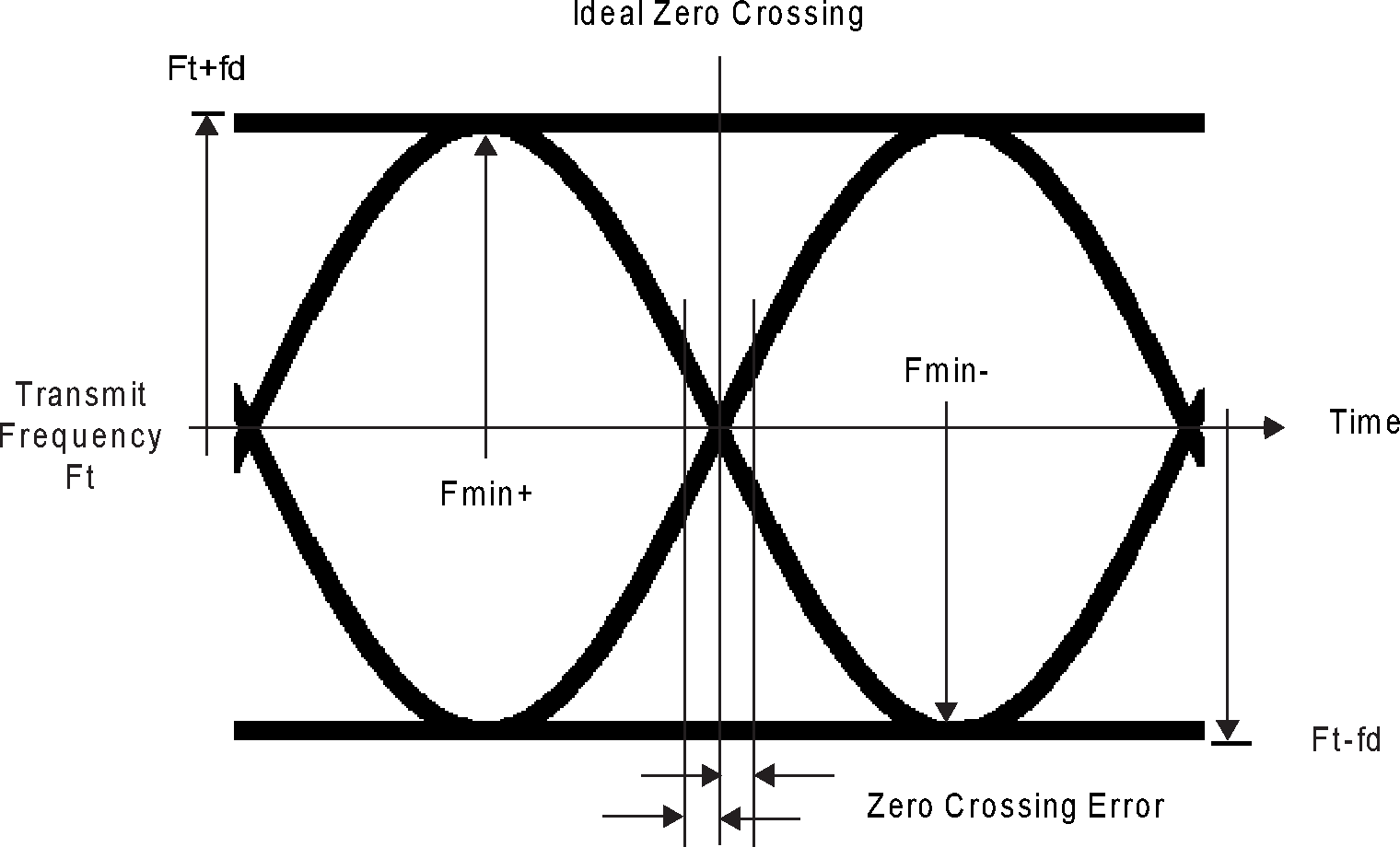
For each transmission, the minimum frequency deviation, Fmin = min{|Fmin+|, Fmin-}, which corresponds to 1010 sequence shall be no smaller than ±80% of the frequency deviation (fd) with respect to the transmit frequency Ft, which corresponds to a 00001111 sequence.
In addition, the minimum frequency deviation shall never be smaller than 115 kHz. The data transmitted has a symbol rate of 1 Msym/s.
The zero crossing error is the time difference between the ideal symbol period and the measured crossing time. This shall be less than ± 1/8 of a symbol period.
See Figure 3.1 for the definitions of some symbols and terms in these requirements.
3.1.2. Spurious emissions
In-band spurious emissions shall be measured with a frequency hopping radio transmitting on one RF channel and receiving on a second RF channel; this means that the synthesizer may change RF channels between reception and transmission, but always returns to the same transmit RF channel. The equipment manufacturer is responsible for compliance in the intended country of use.
3.1.2.1. In-band spurious emission
Within the ISM band the transmitter shall pass a spectrum mask, given in Table 3.2. The spectrum shall comply with the 20 dB bandwidth definition in FCC part 15.247 and shall be measured accordingly. In addition to the FCC requirement an adjacent channel power on adjacent channels with a difference in RF channel number of two or greater is defined. This adjacent channel power is defined as the sum of the measured power in a 1 MHz bandwidth. The transmitted power shall be measured in a 100 kHz bandwidth using maximum hold. The device shall transmit on RF channel M and the adjacent channel power shall be measured on RF channel number N. The transmitter shall transmit a pseudo random data pattern in the payload throughout the test.
Frequency offset | Transmit Power |
|---|---|
± 500 kHz | -20 dBc |
2 MHz (|M-N| = 2) | -20 dBm |
3 MHz or greater (|M-N| ≥ 3) | -40 dBm |
Note
Note: If the output power is less than 0 dBm then, wherever appropriate, the FCC's 20 dB relative requirement overrules the absolute adjacent channel power requirement stated in Table 3.2.
Exceptions are allowed in up to three bands of 1 MHz width centered on a frequency which is an integer multiple of 1 MHz. They shall comply with an absolute value of –20 dBm.
3.1.3. Radio frequency tolerance
The transmitted initial center frequency shall be within ±75 kHz from Fc. The initial frequency accuracy is defined as being the frequency accuracy before any packet information is transmitted.
The frequency drift requirement is not included in the ±75 kHz.
The limits on the transmitter center frequency drift within a packet are specified in Table 3.3. The different packets are defined in the Baseband Specification.
Duration of Packet | Frequency Drift | ||||||||||||||||||||||||||||||||||||||||||||||||
|---|---|---|---|---|---|---|---|---|---|---|---|---|---|---|---|---|---|---|---|---|---|---|---|---|---|---|---|---|---|---|---|---|---|---|---|---|---|---|---|---|---|---|---|---|---|---|---|---|---|
Max length one slot packet | ±25 kHz | ||||||||||||||||||||||||||||||||||||||||||||||||
Max length three slot packet | ±40 kHz | ||||||||||||||||||||||||||||||||||||||||||||||||
Max length five slot packet | ±40 kHz | ||||||||||||||||||||||||||||||||||||||||||||||||
Maximum drift rate[1] | 400 Hz/µs | ||||||||||||||||||||||||||||||||||||||||||||||||
[1] The maximum drift rate is allowed anywhere in a packet. | |||||||||||||||||||||||||||||||||||||||||||||||||
3.2. Enhanced Data Rate
A key characteristic of the Enhanced Data Rate mode is that the modulation mode is changed within the packet. The access code and packet header, as defined in [Vol 2] Part B, Table 6.1, are transmitted with the Basic Rate 1 Mb/s GFSK modulation mode, whereas the subsequent synchronization sequence, payload, and trailer sequence are transmitted using the Enhanced Data Rate PSK modulation mode.
3.2.1. Modulation characteristics
During access code and packet header transmission the Basic Rate GFSK modulation mode shall be used. During the transmission of the synchronization sequence, payload, and trailer sequence a PSK type of modulation with a data rate of 2 Mb/s or optionally 3 Mb/s shall be used. The following subsections specify the PSK modulation for this transmission.
3.2.1.1. Modulation method overview
The PSK modulation format defined for the 2 Mb/s transmission shall be π/4 rotated differential encoded quaternary phase shift keying (π/4-DQPSK).
The PSK modulation format defined for the 3 Mb/s transmission shall be differential encoded 8-ary phase shift keying (8DPSK).
The modulation shall employ square-root raised cosine pulse shaping to generate the equivalent lowpass information-bearing signal v(t). The output of the transmitter shall be a bandpass signal that can be represented as
with Fc denoting the carrier frequency.
3.2.1.2. Differential phase encoding
For the M-ary modulation, the binary data stream {bn}, n=1,2,3, ...N, shall be mapped onto a corresponding sequence {Sk}, k=1,2, ...N/log2(M) of complex valued signal points. M=4 applies for 2 Mb/s and M=8 applies for 3 Mb/s. Gray coding shall be applied as shown in Table 3.4 and Table 3.5. In the event that the length of the binary data stream N is not an integer multiple of log2(M), the last symbol of the sequence {Sk} shall be formed by appending data zeros to the appropriate length. The signal points Sk shall be defined by:
The relationship between the binary input bk and the phase shall be as defined in Table 3.4 for the 2 Mb/s transmission and in Table 3.5 for the 3 Mb/s transmission.
b2k-1 | b2k | k |
|---|---|---|
0 | 0 | π/4 |
0 | 1 | 3π/4 |
1 | 1 | -3π/4 |
1 | 0 | -π/4 |
b3k-2 | b3k-1 | 3k | k |
|---|---|---|---|
0 | 0 | 0 | 0 |
0 | 0 | 1 | π/4 |
0 | 1 | 1 | π/2 |
0 | 1 | 0 | 3π/4 |
1 | 1 | 0 | π |
1 | 1 | 1 | -3π/4 |
1 | 0 | 1 | -π/2 |
1 | 0 | 0 | -π/4 |
3.2.1.3. Pulse shaping
The lowpass equivalent information-bearing signal v(t) shall be generated according to
in which the symbol period T shall be 1 µs.
The frequency spectrum P(f), which corresponds to the square-root raised cosine pulse p(t) of the pulse shaping filter is:
The roll off factor β shall be 0.4.
3.2.1.4. Modulation accuracy
The measurement of modulation accuracy utilizes differential error vector magnitude (DEVM) with tracking of the carrier frequency drift. The definition of DEVM and the derivation of the RMS and peak measures of DEVM are given in Appendix C.
The DEVM shall be measured over the synchronization sequence and payload portions of the packet, but not the trailer symbols. For each modulation method and each measurement carrier frequency, the DEVM measurement is made over a total of 200 non-overlapping blocks, where each block contains 50 symbols.
The transmitted packets shall be the longest supported packet type for each modulation method, as defined in [Vol 2] Part B, Table 6.8 and [Vol 2] Part B, Table 6.9.
The DEVM is measured using a square-root raised cosine filter, with a roll-off of 0.4 and a 3 dB bandwidth of ±500 kHz.
3.2.1.4.1. RMS DEVM
The RMS DEVM for any of the measured blocks shall not exceed 0.20 for π/4-DQPSK and 0.13 for 8DPSK.
3.2.1.4.2. 99% DEVM
The 99% DEVM (defined as the DEVM value for which 99% of measured symbols have a lower DEVM) shall not exceed 0.30 for π/4-DQPSK and 0.20 for 8DPSK.
3.2.1.4.3. Peak DEVM
The Peak DEVM shall not exceed 0.35 for π/4-DQPSK and 0.25 for 8DPSK.
3.2.2. Spurious emissions
In-band spurious emissions shall be measured with a frequency hopping radio transmitting on one RF channel and receiving on a second RF channel; this means that the synthesizer may change RF channels between reception and transmission, but always returns to the same transmit RF channel. The equipment manufacturer is responsible for compliance in the intended country of use.
3.2.2.1. In-band spurious emission
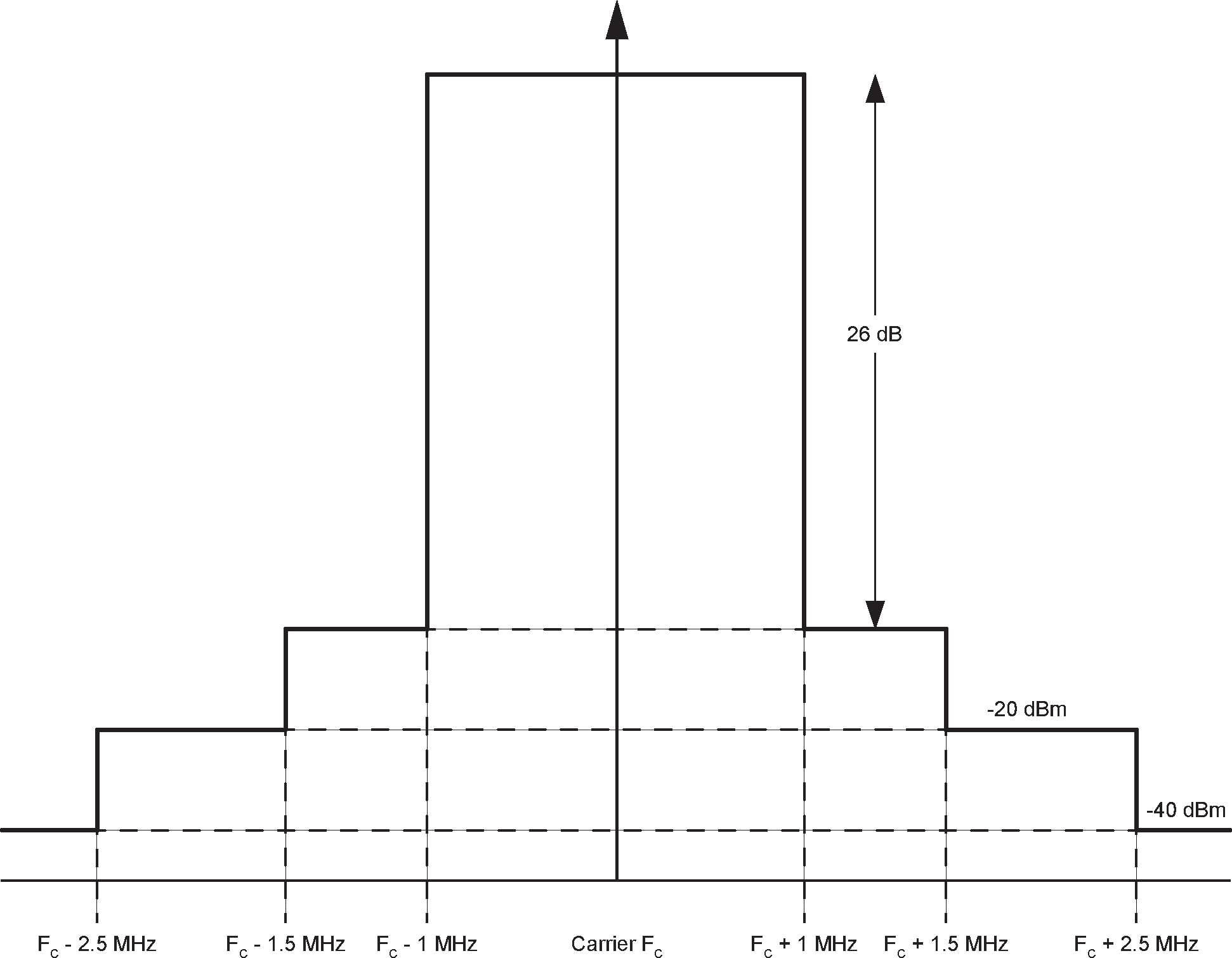
Within the ISM band the power spectral density of the transmitter shall comply with the following requirements when sending pseudo random data. All power measurements shall use a 100 kHz bandwidth with maximum hold. The power measurements between 1 MHz and 1.5 MHz from the carrier shall be at least 26 dB below the maximum power measurement up to 500 kHz from the carrier. The adjacent channel power for channels at least 2 MHz from the carrier is defined as the sum of the power measurements over a 1 MHz channel and shall not exceed -20 dBm for the second adjacent channels and -40 dBm for the third and subsequent adjacent channels. These requirements shall apply to the transmitted signal from the start of the guard time to the end of the power down ramp. The spectral mask is illustrated in Figure 3.2.
Exceptions are allowed in up to 3 bands of 1 MHz width centered on a frequency which is an integer multiple of 1 MHz. They shall comply with an absolute value of –20 dBm.
3.2.3. Radio frequency tolerance
The same carrier frequencies Fc as used for Basic Rate transmissions shall be used for the Enhanced Data Rate transmissions. The transmitted initial center frequency accuracy shall be within ±75 kHz from Fc. The maximum excursion from Fc (frequency offset plus drift) shall not exceed ±75 kHz.
The initial frequency accuracy is defined as being the frequency accuracy before any information is transmitted.
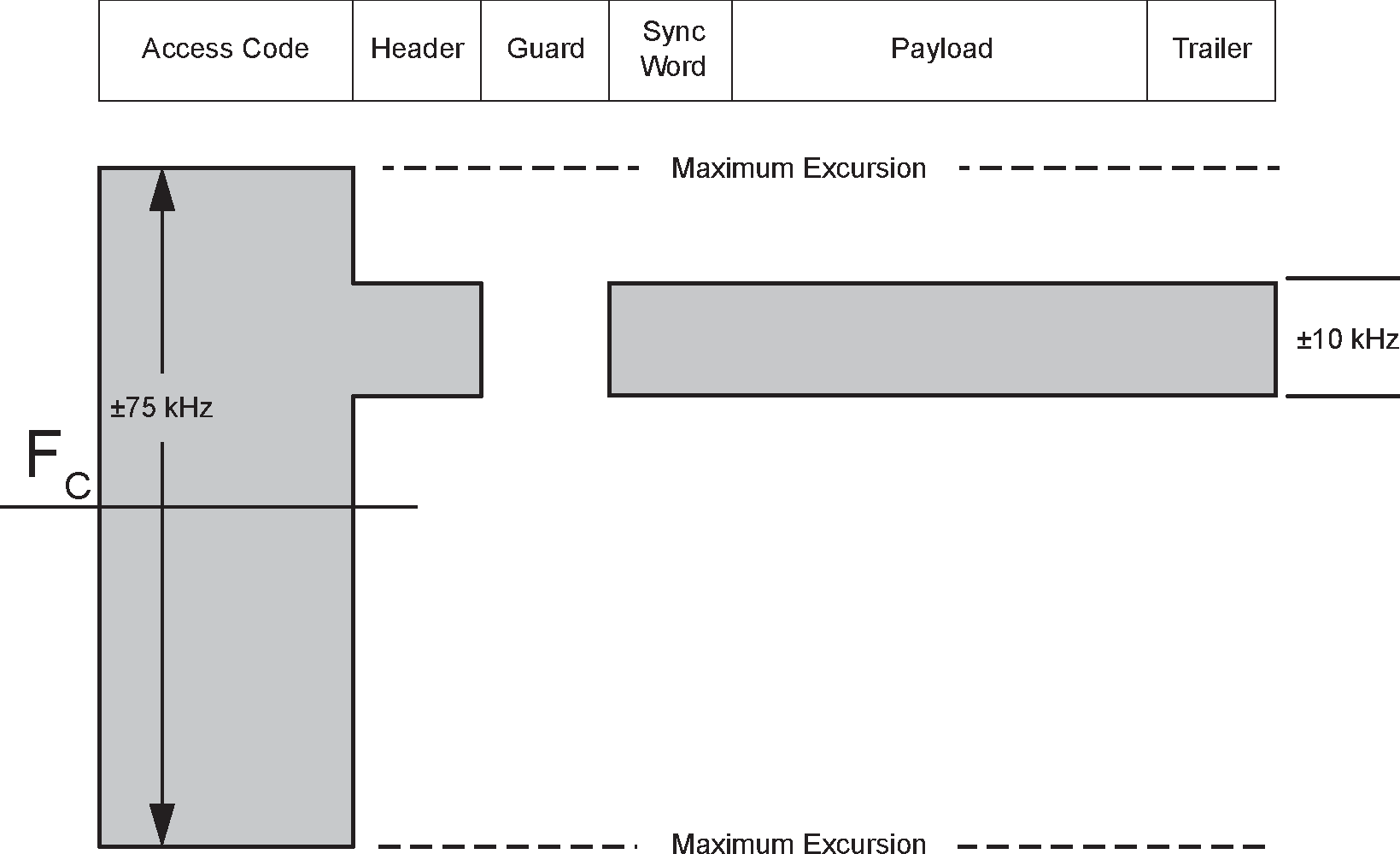
The requirements on accuracy and stability are illustrated by Figure 3.3 for the Enhanced Data Rate packet format defined in Definition: Baseband Specification . The higher frequency accuracy requirement shall start at the first symbol of the header. The maximum drift over the header, synchronization sequence and payload shall be ±10 kHz.
3.2.4. Relative transmit power
The requirement on the relative power of the GFSK and DPSK portions of the Enhanced Data Rate packet is defined as follows. The average power level during the transmission of access code and header is denoted as PGFSK and the average power level during the transmission of the synchronization sequence and the payload is denoted as PDPSK. The following inequalities shall be satisfied independently for each Enhanced Data Rate packet transmitted:
(PGFSK - 4 dB) < PDPSK < (PGFSK + 1 dB)
4. Receiver characteristics
The receiver characteristics shall be measured using loopback as defined in [Vol 3] Part D, Section 1.
The reference sensitivity level referred to in this section is -70 dBm.
4.1. Basic Rate
4.1.1. Actual sensitivity level
The actual sensitivity level is defined as the input level for which a raw bit error rate (BER) of 0.1% is met. The receiver sensitivity shall be below or equal to –70 dBm with any Bluetooth transmitter compliant to the transmitter specification specified in Section 3.
4.1.2. Interference performance
The interference performance on Co-channel and adjacent 1 MHz and 2 MHz shall be measured with the wanted signal 10 dB over the reference sensitivity level. For interference performance on all other RF channels the wanted signal shall be 3 dB over the reference sensitivity level. If the frequency of an interfering signal is outside of the band 2400 MHz to 2483.5 MHz, the out-of-band blocking specification (see Section 4.1.3) shall apply. The interfering signal shall be Bluetooth-modulated (see Section 4.1.7). The BER shall be ≤0.1% for all the signal-to-interference ratios listed in Table 4.1:
Frequency of Interference | Ratio | ||||||||||||||||||||||||||||||||||||||||||||||||
|---|---|---|---|---|---|---|---|---|---|---|---|---|---|---|---|---|---|---|---|---|---|---|---|---|---|---|---|---|---|---|---|---|---|---|---|---|---|---|---|---|---|---|---|---|---|---|---|---|---|
Co-Channel interference, C/Ico-channel | 11 dB | ||||||||||||||||||||||||||||||||||||||||||||||||
Adjacent (1 MHz) interference[1], C/I1 MHz | 0 dB | ||||||||||||||||||||||||||||||||||||||||||||||||
Adjacent (2 MHz) interference[1], C/I2 MHz | -30 dB | ||||||||||||||||||||||||||||||||||||||||||||||||
Adjacent (≥3 MHz) interference[1], C/I≥3 MHz | -40 dB | ||||||||||||||||||||||||||||||||||||||||||||||||
-9 dB | |||||||||||||||||||||||||||||||||||||||||||||||||
Adjacent (1 MHz) interference to in-band image frequency[1], C/IImage±1MHz | -20 dB | ||||||||||||||||||||||||||||||||||||||||||||||||
[1] If two adjacent channel specifications from Table 4.1 are applicable to the same channel, the more relaxed specification applies. [2] In-band image frequency [3] If the image frequency ≠ n*1 MHz, then the image reference frequency is defined as the closest n*1 MHz frequency for integer n. | |||||||||||||||||||||||||||||||||||||||||||||||||
These specifications are only to be tested at nominal temperature conditions with a device receiving on one RF channel and transmitting on a second RF channel; this means that the synthesizer may change RF channels between reception and transmission, but always returns to the same receive RF channel.
RF channels where the requirements are not met are called spurious response RF channels. Five spurious response RF channels are allowed at RF channels with a distance of ≥2 MHz from the wanted signal. On these spurious response RF channels a relaxed interference requirement C/I = -17 dB shall be met.
4.1.3. Out-of-band blocking
The out-of-band suppression (or rejection) shall be measured with the wanted signal 3 dB over the reference sensitivity level. The interfering signal shall be a continuous wave signal. The BER shall be ≤0.1%. The out-of-band blocking shall fulfil the following requirements:
Interfering Signal Frequency | Interfering Signal Power Level |
|---|---|
30 MHz to 2000 MHz | -10 dBm |
2000 MHz to 2399 MHz | -27 dBm |
2484 MHz to 3000 MHz | -27 dBm |
3000 MHz to 12.75 GHz | -10 dBm |
24 exceptions are permitted which are dependent upon the given RF channel and are centered at a frequency which is an integer multiple of 1 MHz. For at least 19 of these spurious response frequencies, a reduced interference level of at least -50 dBm is allowed in order to achieve the required BER = 0.1% performance, whereas for a maximum of 5 of the spurious frequencies the interference level may be assumed arbitrarily lower.
4.1.4. Intermodulation characteristics
The reference sensitivity performance, BER = 0.1%, shall be met under the following conditions:
The wanted signal shall be at frequency f0 with a power level 6 dB over the reference sensitivity level.
A static sine wave signal shall be at a frequency f1 with a power level of –39 dBm.
A Bluetooth modulated signal (see Section 4.1.7) shall be at f2 with a power level of -39 dBm.
Frequencies f0, f1 and f2 shall be chosen such that and , where n can be 3, 4, or 5. The system shall fulfill at least one of the three alternatives (n=3, 4, or 5).
4.1.5. Maximum usable level
The maximum usable input level that the receiver operates at shall be greater than -20 dBm. The BER shall be less than or equal to 0.1% at –20 dBm input power.
4.1.6. Received Signal Strength Indication
If a device supports Received Signal Strength Indication (RSSI) the accuracy shall be ±6 dB. If the device is aware that the RSSI varies across frequencies, then it should update the RSSI value of a packet depending on the frequency that the packet was received on before using the value, e.g., before reporting it to the Host.
4.1.7. Reference signal definition
A Bluetooth modulated interfering signal shall be defined as:
Modulation = GFSK Modulation index = 0.32±1% BT= 0.5±1% Bit Rate = 1 Mb/s ±1 ppm Modulating Data for wanted signal = PRBS9 Modulating Data for interfering signal = PRBS15 Frequency accuracy better than ±1 ppm.
4.2. Enhanced Data Rate
4.2.1. Actual sensitivity level
The actual sensitivity level shall be defined as the input level for which a raw bit error rate (BER) of 0.01% is met. The requirement for a Bluetooth π/4-DQPSK and 8DPSK Enhanced Data Rate receiver shall be an actual sensitivity level of –70 dBm or better. The receiver shall achieve the –70 dBm sensitivity level with any Bluetooth transmitter compliant to the Enhanced Data Rate transmitter specification as defined in Section 3.2.
4.2.2. BER floor performance
The receiver shall achieve a BER less than 0.001% at 10 dB above the reference sensitivity level.
4.2.3. Interference performance
The interference performance for co-channel and adjacent 1 MHz and 2 MHz channels shall be measured with the wanted signal 10 dB above the reference sensitivity level. On all other frequencies the wanted signal shall be 3 dB above the reference sensitivity level. The requirements in this section shall only apply if the frequency of the interferer is inside of the band 2400 MHz to 2483.5 MHz.
The interfering signal for co-channel interference shall be similarly modulated as the desired signal. The interfering signal for other channels shall be equivalent to a nominal Bluetooth Basic Rate GFSK transmitter. The interfering signal shall carry random data.
A BER of 0.1% or better shall be achieved for the signal to interference ratios defined in Table 4.3.
Frequency of Interference | π/4-DQPSK Ratio | 8DPSK Ratio | |||||||||||||||||||||||||||||||||||||||||||||||
|---|---|---|---|---|---|---|---|---|---|---|---|---|---|---|---|---|---|---|---|---|---|---|---|---|---|---|---|---|---|---|---|---|---|---|---|---|---|---|---|---|---|---|---|---|---|---|---|---|---|
Co-Channel interference, C/I co-channel | 13 dB | 21 dB | |||||||||||||||||||||||||||||||||||||||||||||||
Adjacent (1 MHz) interference[1], C/I1 MHz | 0 dB | 5 dB | |||||||||||||||||||||||||||||||||||||||||||||||
Adjacent (2 MHz) interference[1], C/I2 MHz | -30 dB | -25 dB | |||||||||||||||||||||||||||||||||||||||||||||||
Adjacent (≥3 MHz) interference[1] | -40 dB | -33 dB | |||||||||||||||||||||||||||||||||||||||||||||||
-7 dB | 0 dB | ||||||||||||||||||||||||||||||||||||||||||||||||
Adjacent (1 MHz) interference to in-band image frequency[1],[2],[3], C/IImage ±1 MHz | -20 dB | -13 dB | |||||||||||||||||||||||||||||||||||||||||||||||
[1] If two adjacent channel specifications from Table 4.3 are applicable to the same channel, the more relaxed specification applies. [2] In-band image frequency. [3] If the image frequency is not equal to n*1 MHz, then the image reference frequency is defined as the closest n*1 MHz frequency for integer n. | |||||||||||||||||||||||||||||||||||||||||||||||||
These specifications are only to be tested at nominal temperature conditions with a receiver hopping on one frequency; this means that the synthesizer may change frequency between receive slot and transmit slot, but always returns to the same receive frequency.
Frequencies where the requirements are not met are called spurious response frequencies. Five spurious response frequencies are allowed at frequencies with a distance of ≥2 MHz from the wanted signal. On these spurious response frequencies a relaxed interference requirement C/I = -15 dB for π/4-DQPSK and C/I = -10 dB for 8DPSK shall be met.
4.2.4. Maximum usable level
The maximum usable input level that the receiver operates at shall be greater than -20 dBm. The BER shall be less than or equal to 0.1% at -20 dBm input power.
4.2.5. Out-of-band and intermodulation characteristics
The Basic Rate out-of-band blocking and intermodulation requirements also apply to Enhanced Data Rate since they result in adequate performance. No additional requirements apply to Enhanced Data Rate.
4.2.6. Reference signal definition
A 2 Mb/s Bluetooth signal used as "wanted" or "interfering signal" is defined as:
Modulation = π/4-DQPSK |
Symbol Rate = 1 Msym/s ± 1 ppm |
Frequency accuracy better than ±1 ppm |
Modulating Data for wanted signal = PRBS9 |
Modulating Data for interfering signal = PRBS15 |
RMS Differential Error Vector Magnitude < 5% |
Average power over the GFSK and DPSK portions of the packet shall be equal to within ±1 dB |
A 3 Mb/s Bluetooth signal used as "wanted" or "interfering signal" is defined as:
Modulation = 8DPSK |
Symbol Rate = 1 Msym/s ± 1 ppm |
Frequency accuracy better than ±1 ppm |
Modulating Data for wanted signal = PRBS9 |
Modulating Data for interfering signal = PRBS15 |
RMS Differential Error Vector Magnitude < 5% |
Average power over the GFSK and DPSK portions of the packet shall be equal to within ±1 dB |
Appendix A. Test conditions
A.1. Nominal test conditions
A.1.1. Nominal temperature
The nominal temperature conditions for tests shall be +15 to +35 °C. When it is impractical to carry out the test under this condition a note to this effect, stating the ambient temperature, shall be recorded. The actual value during the test shall be recorded in the test report.
A.1.2. Nominal power source
The normal test voltage for the equipment shall be the nominal voltage for which the equipment was designed.
A.2. [This section is no longer used]
Appendix B. [This Appendix is no longer used]
Appendix C. Modulation accuracy definition
C.1. Enhanced Data Rate modulation accuracy
The Enhanced Data Rate modulation accuracy is defined by the differential error vector, being the difference between the vectors representing consecutive symbols of the transmitted signal, after passing the signal through a specified measurement filter, sampling it at the symbol rate with an optimum sampling phase and compensating it for carrier frequency error and for the ideal carrier phase changes. The magnitude of the normalized differential error vector is called the Differential Error Vector Magnitude (DEVM). The objective of the DEVM is to estimate the modulation errors that would be perceived by a differential receiver.
In an ideal transmitter, the input bit sequence {bj} is mapped onto a complex valued symbol sequence {Sk}. Subsequently, this symbol sequence is transformed into a baseband signal S(t) by means of a pulse-shaping filter.
In an actual transmitter implementation, the bit sequence {bj} generates a baseband equivalent transmitted signal Y(t). This signal Y(t) contains, besides the desired component S(t), multiple distortion components. This is illustrated in Figure C.1 (in Figure C.1 and Figure C.2 a circle with an X indicates a mixer).
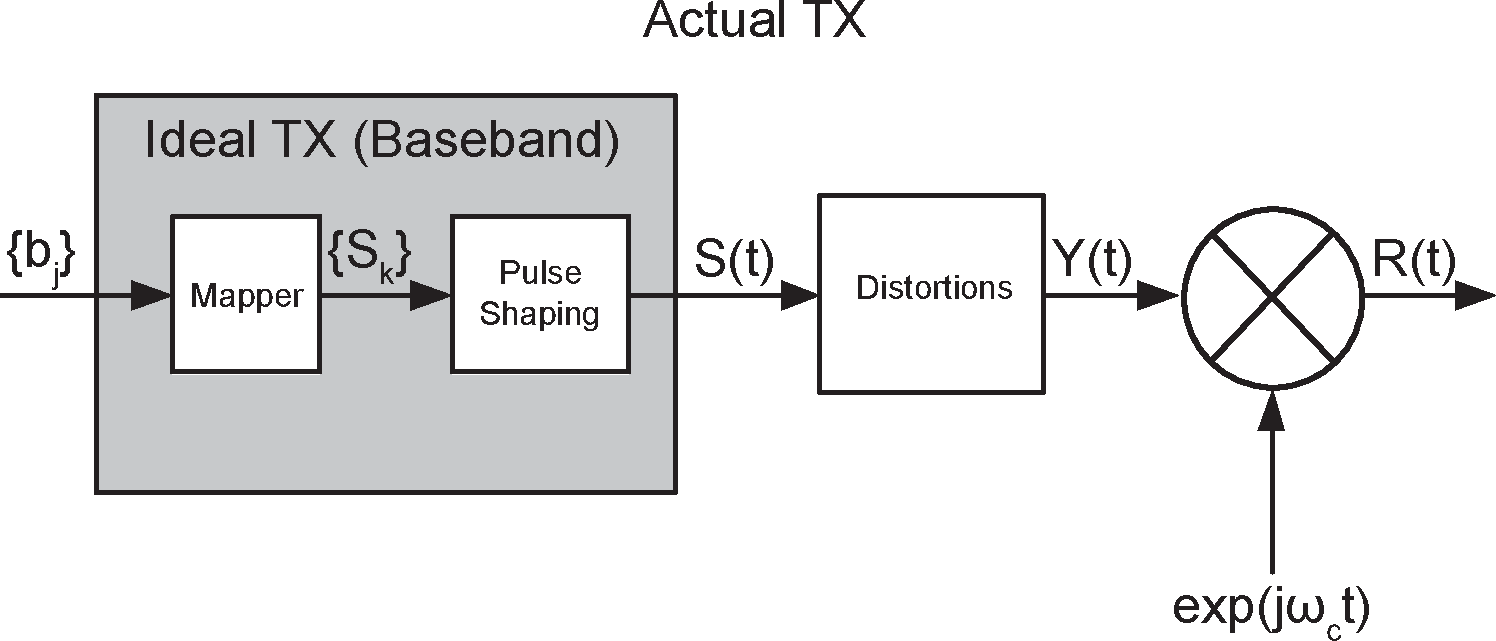
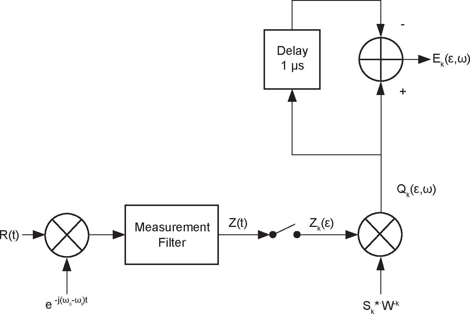
Let Z(t) be the output of the measurement filter after first compensating the received signal for the initial center frequency error, ωi, of the received packet, i.e. the output after down conversion and filtering the transmit signal R(t) (see Figure C.2).The measurement filter is defined by a square-root raised cosine shaping filter with a roll-off factor equal to 0.4 and 3 dB bandwidth of ±500 kHz.
Let {Zk(ε)} be the sequence of samples obtained by sampling the signal Z(t) with a sampling period equal to the symbol period T and a sampling phase equal to ε such that Zk(ε)=Z((k+ε)T).
This sequence {Zk(ε)} would coincide with the symbol sequence {Sk} if no distortion is present and the correct timing phase ε is chosen.
To reflect the behavior of a typical differential receiver, the sample sequence {Zk(ε)} should be compensated for carrier frequency drift. Therefore, the sequence {Zk(ε)} is multiplied by a factor W-k in which W = ejωT accounts for the frequency offset ω. A constant value of ω is used for each DEVM block of N = 50 symbols, but ω may vary between DEVM blocks (the values of ω can be used to measure carrier frequency drift).
In addition, {Zk(ε)} is compensated for the ideal phase changes between symbols by multiplying it with the complex conjugate of the symbol sequence {Sk}. However, it is not necessary to compensate {Zk(ε)} for initial carrier phase or output power of the transmitter.
Let {Qk(ε,ω)} denote the compensated sequence {Zk(ε)}, where the ideal phase changes have been removed and ε and ω are chosen optimally to minimize the DEVM, (i.e. remove time and frequency uncertainty). For a transmitter with no distortions other than a constant frequency error, {Qk(ε,ω)} is a complex constant that depends on the initial carrier phase and the output power of the transmitter.
The differential error sequence {Ek(ε,ω)} is defined as the difference between {Qk(ε,ω)} and {Qk-1(ε,ω)}. This reflects the modulation errors that would be perceived by a differential receiver. For a transmitter with no distortions other than a constant frequency error, {Ek(ε,ω)} is zero.
The definitions of the DEVM measures are based upon this differential error sequence {Ek(ε,ω)}. The generation of the error sequence is depicted in Figure C.2 (the circle with the + indicates a direct summation function; the input with the "−" is negated before being summed).
C.1.1. RMS DEVM
The root mean squared DEVM (RMS DEVM) computed over N = 50 symbols is defined as:
As can be seen from the expression above, the RMS DEVM is the square-root of the normalized power of the error.
C.1.2. Peak DEVM
The DEVM at symbol k is defined as:
where ε0 and ω0 are the values for ε and ω used to calculate the RMS DEVM.
The peak DEVM is defined as: